📝 Personal Notes
Computer Engineering
This notebook largely collects tutorial material I wrote for myself while learning about how computers work (specifically computer processors) and how I can build them from the ground up. My special interest is not just in understanding the basics of CPUs but rather, I want to learn how to take any application and make a computer for it.
Hacking Together a Tiny Computer
The first ever book that I read on this topic was "The Elements of Computing Systems: Building a Modern Computer from First Principles" by Noam Nisan and Shimon Schocken which I used to build a simple Hack computer starting with only logic gates. I partly document this journy in my Computer Basics: NAND to Pong notes.
There is also a free course called "NAND to Tetris" with lots of free related material out there which has a very active community of enthusiasts building this computers with various fun twists and implementing various applications on it. This gives us a concrete yet basic understanding of all the core elements of a computer from logic gates up to the operating system.
The book "Digital Design and Computer Architecture" by Sarah L. and David Money Harris complements this learning program quite well, too. Personally, I think building a 6502 computer and designing your own PCB for it is a cool retro-tech project.
If you want to build an actual bread board computer, check out Ben Eater's videos and material!
Princeton's Computer Architecture Course
To go deeper and learn how to create modern processors, not toy chips, not decades old chips, but processors that one would find in today's computers, I then continued to work through Princeton's lectures on computer architecture which are also freely available online.
The course is heavily inspired by the book "Computer Architecture: A Quantitative Approach" by John L. Hennessy and David A. Patterson.
The textbook "Modern Processor Design: Fundamentals of Superscalar Processors" by John Paul Shen and Mikko H. Lipasti is also recommended during this course as well but I have yet to take a better look at it.
Onur Mutlu Lectures
Additionally, I find professor Mutlu's lectures on computers and computer architectures highly valuable. While I am writing this, I am not focused on them though. This is a mere note to my future self to go back to his work and try to integrate it with everything I will have learned.
Analog Computing
I have much to say about analog computing since I've had several phases of obsession regarding it. But more at a later time.
Exotic Computing
The same holds true for the various other computing approaches like photonic computing, quantum computing, reversible computing, and so on.
"On the one hand, the Hack [general computer] architecture can be built in just a few hours of work, [...] at the same time, Hack is sufficiently general to illustrate the key operating principles and hardware elements underlying the design of any digital computer." Elements of Computing Systems (ECS). I recommend getting this book. But it can be helpful to hence also look into the related NAND to Tetris course.
If you want to learn how to design a Hack computer and do all of the above, I documented every step of the process in the chapters below. This is not a guide to solve the famous NAND-to-Tetris course challenges. I barely skimmed the book and didn't look at the course much.
- Overview. This is where you are right now.
- Get Started. Explains what we are going to do and guides you through the setup of all the tools. We'll end by writing a "Hello World!" of Verilog and simulating/testing it.
- Boolean Arithmetic. Here, we'll create our first arithmetic modules, starting with a Half-Adder and ending with a complete, working Arithmetic Logic Unit (ALU).
- Sequential Logic. This chapter contains the code and notes for building registers for memory as well as a counter.
- Machine Language. This is where we'll write our first little program making use of the components we defined up to this point.
- Computer Architecture. We'll then finally put everything together, designing the whole hardware architecture of the computer containing, memory, instruction memory, and the CPU.
- Assembler. Finally, we'll write some Assembly for this computer concluding in an implementation of the game Pong.
Get Started
If you actually want to work through this and build your own Hack computer similar to how I did it, we'll first need to set up our development environment. Feel free to skip this if you already understand Verilog and you're just want to read/browse a little
Tools
Only a few tools are necessary. We use
- Visual Studio Code and
- Verilog HDL to program the designs,
- Icarus Verilog for simulation as it is easier to install than Verilator on Windows, and
- GTKWave for waveform viewing.
- And Python for simple scripts like the assembler.
Optionally, Logisim can be a nice playground to test circuit ideas fast.
Installing Logisim
Installing Logisim is as easy as downloading the .exe from http://www.cburch.com/logisim/ and following the install instructions. It is a compiled program with an intuitive GUI. You can then go ahead and immediately build your first digital circuits. In fact, Logisim is quite capable of simulating any computer you want to build. But while it is more intuitive and great for testing ideas, it is also quite time-consuming for larger projects to draw and connect every component yourself. That's just one of many reasons for why we have programmatic hardware description languages.
Installing Icarus Verilog & GTK Wave
Download Icarus here. This installation program will include gtkwave as well. Make sure to use the most recent version and during installation check the installation path box so that you can open Icarus and verilog simply by typing
>gtkwave
which opens a nice little GUI which we'll discuss later or
>iverilog
which will just print out some text in your terminal. This video might be of great help to you and it also shows you how to write, simulate, and visualize the signals of your Verilog modules. It really is that simple. The whole ecosystem simply has terrible, terrible documentation.
The Basic Workflow
The workflow overall using these tools is pretty straightforward and we'll repeat it over and over.
Step 1: Create a Verilog file. We'll call this one test.v:
module myModule();

initial
  begin
    $display("Hello World!");   // This will display a message
    $finish ; // This causes the simulation to end.  Without, it would go on..and on.
  end

endmodule
This module simply prints out the classic "Hello World!". Great!
Step 2. We compile the .v file using Icarus:
>iverilog -o test.vvp test.v
The -o switch assigns a name to the output object file. Without this switch the output file would be called a.out. The hello.v indicates the source file to be compiled. There should be practically no output when you compile this source code, unless there are errors.
Step 3. You are ready to simulate this Hello World verilog program. To do so, invoke as such:
>vvp test.vvp
Hello World!
Now, inside Visual Studio Code you can install the Verilog HDL extension which adds a little green button at the top of the window which helps you compile your verilog code instead of you having to type the command out in the terminal every time.
Step 4. Visualize the waveforms/signals in gtkwave to check if our module functions as desired. To create and visualize waveforms, modify your Verilog code to include signal declarations and generate a VCD (Value Change Dump) file. Let's take for example the following Verilog:
module myModule();
  reg clk;  // Declare a clock signal
  reg [3:0] counter;  // Declare a 4-bit counter

  initial begin
    $dumpfile("test.vcd");  // Create a VCD file named test.vcd
    $dumpvars(0, myModule);  // Dump all variables in the module

    clk = 0;
    counter = 0;

    repeat(16) begin
      #5 clk = ~clk;  // Toggle clock every 5 time units
      if (clk) counter = counter + 1;  // Increment counter on rising edge
    end

    $display("Simulation complete");
    $finish;
  end
endmodule
Compile and run the simulation as before:
>iverilog -o test.vvp test.v
>vvp test.vvp
which now also creates the test.vcd file. Which we can then view with
>gtkwave test.vcd
opening the GTKView software. Select the waveform in the UI and you'll see something like this:
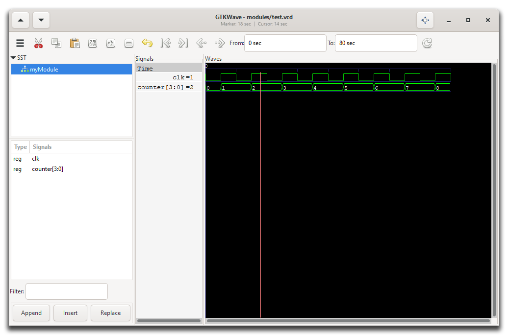 |
|---|
GTKWave program showing the test.vcd waveform. |
A Short Introduction to Verilog
Verilog is a hardware description language (HDL) used to model digital electronic systems. It can be used to describe hardware at various levels of abstraction, from high-level behavioral descriptions to low-level gate-level implementations allowing designers to simulate and synthesize digital circuits as hinted at before.
As we already saw as well, the basic unit of design in Verilog is a module which can represent anything from simple print statement or gate to highly complex systems. It has
- a port list (inputs and outputs)
- and a body describing its functionality.
Verilog has two main data types: nets (like wires) and registers.
Common keywords are: wire, reg, integer, real, time.
Vectors can be declared to represent multiple bits (e.g., wire [7:0] bus;).
In this case, we have an 8-bit bus.
And importantly, there are various operations Verilog defines.
Bitwise operators:
&: Bitwise AND - Performs a bitwise AND operation between corresponding bits of two operands. Each bit of the result is set to 1 if both corresponding bits of the operands are 1.|: Bitwise OR - Performs a bitwise OR operation between corresponding bits of two operands. Each bit of the result is set to 1 if at least one of the corresponding bits of the operands is 1.^: Bitwise XOR - Performs a bitwise exclusive OR (XOR) operation between corresponding bits of two operands. Each bit of the result is set to 1 if only one of the corresponding bits is 1.~: Bitwise NOT - Performs a bitwise negation (complement) of the operand. It inverts each bit of its operand.
Logical operators:
&&: Logical AND - Returns true if both operands are non-zero (true), otherwise returns false. Unlike &, it operates on entire expressions, not individual bits.||: Logical OR - Returns true if at least one of the operands is non-zero (true). Similar to &&, it operates on entire expressions.!: Logical NOT - Returns true if the operand is zero (false), otherwise returns false. It inverts the boolean value of its operand.
Arithmetic operators:
+: Addition - Adds two operands.-: Subtraction - Subtracts the second operand from the first.*: Multiplication - Multiplies two operands./: Division - Divides the first operand by the second operand. Note that in Verilog, division of integers results in integer division.%: Modulus - Returns the remainder after division of the first operand by the second.
Relational operators:
==: Equality - Returns true if both operands are equal.!=: Inequality - Returns true if the operands are not equal.<: Less Than - Returns true if the first operand is less than the second.>: Greater Than - Returns true if the first operand is greater than the second.<=: Less Than or Equal To - Returns true if the first operand is less than or equal to the second.>=: Greater Than or Equal To - Returns true if the first operand is greater than or equal to the second.
Shift operators:
<<: Logical Left Shift - Shifts the bits of the first operand to the left by the number of positions specified by the second operand. Zeroes are shifted into the lower bits.>>: Logical Right Shift - Shifts the bits of the first operand to the right by the number of positions specified by the second operand. Zeroes are shifted into the higher bits.
Concatenation operator:
{}: Concatenation - Combines multiple values or vectors into a single vector. For example, {A, B} concatenates the values A and B into a larger bit vector.
As I mentioned, we can define quite complex modules. Indeed, there are three different paradigms for how to do so: Procedural Blocks, Behavioral Constructs, and Structural Constructs. But more about that later.
Verilog supports specifying delays and timing constraints where symbol is used for delays in simulation.
Here is a simple example of a more practical Verilog module:
module d_flip_flop (
    input clk,    // Clock input
    input d,      // Data input
    output reg q  // Output
);

always @(posedge clk) begin
    q <= d;
end

endmodule
It describes a D flip-flop that updates its output q with the value of input d on the rising edge of the clock signal clk. So we have two inputs (clk, d) and one output (q). The reg defines the data type as a register. A reg can hold a value between assignments, unlike a wire which does not store values.
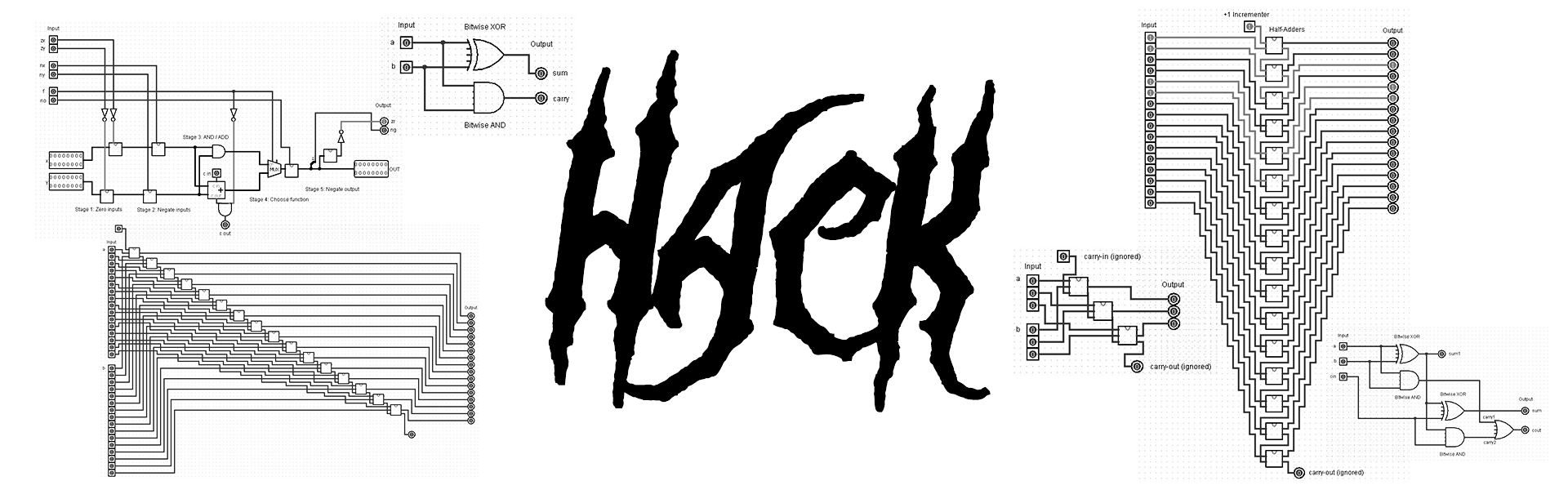
Boolean Arithmetic
Let's build up the individual modules which are typical for ALUs within CPUs, step-by-step. Note that the HACK architecture is extremely simplified. Compare the Verilog I show below to that of other designs and you'll quickly notice the simplicity.
Open the logic.circ Logisim file from the root directory to try out and experiment with the circuits I present here.
Half-Adder
A half-adder is a digital circuit that adds two single binary digits and produces a sum and a carry. The sum is the XOR of the inputs, while the carry is the AND of the inputs.
Truth table for a half-adder:
| Input A | Input B | Sum | Carry |
|---|---|---|---|
| 0 | 0 | 0 | 0 |
| 0 | 1 | 1 | 0 |
| 1 | 0 | 1 | 0 |
| 1 | 1 | 0 | 1 |
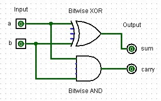 |
|---|
| A half-adder design created in Logisim with two input bits, two output bits, one bitwise XOR and one bitwise AND logic gate. |
module half_adder(
    input a, b,
    output sum, carry
);
    assign sum = a ^ b;
    assign carry = a & b;
endmodule
Let's test this baby to see if it actually does what it is supposed to do. For that, we add a little testbench to our previous code like this
module half_adder(
    input a, b,
    output sum, carry
);
    assign sum = a ^ b;
    assign carry = a & b;
endmodule

// Testbench
module half_adder_tb;
    // Declare signals
    reg a, b;
    wire sum, carry;

    // Instantiate the half adder
    half_adder ha1 (.a(a), .b(b), .sum(sum), .carry(carry));

    // Generate VCD file
    initial begin
        $dumpfile("modules/half_adder.vcd");
        $dumpvars(0, half_adder_tb);

        // Test cases
        a = 0; b = 0; #10;
        a = 0; b = 1; #10;
        a = 1; b = 0; #10;
        a = 1; b = 1; #10;

        $finish;
    end

    // Display results
    initial begin
        $monitor("Time=%0t a=%b b=%b sum=%b carry=%b", $time, a, b, sum, carry);
    end
endmodule
Follow the steps for using GTKWave of the previous chapter and you'll see a return in the terminal and a waveform like this:
VCD info: dumpfile half_adder.vcd opened for output.
Time=0 a=0 b=0 sum=0 carry=0
Time=10 a=0 b=1 sum=1 carry=0
Time=20 a=1 b=0 sum=1 carry=0
Time=30 a=1 b=1 sum=0 carry=1
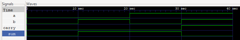 |
|---|
GTKWave snapshot of the signals returned from the half_adder.v testbench. |
Does that make sense? Yes! Great. Let's move on to the next module.
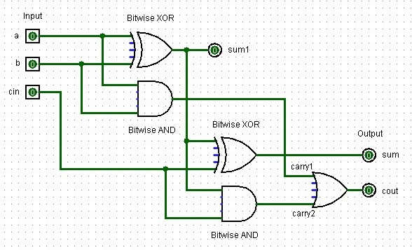
Full-Adder
A full-adder adds three single binary digits (two inputs and one carry-in) and produces a sum and a carry-out. It's implemented using two half-adders and an OR gate.
Truth table for a full-adder:
| Input A | Input B | Carry In | Sum | Carry Out |
|---|---|---|---|---|
| 0 | 0 | 0 | 0 | 0 |
| 0 | 0 | 1 | 1 | 0 |
| 0 | 1 | 0 | 1 | 0 |
| 0 | 1 | 1 | 0 | 1 |
| 1 | 0 | 0 | 1 | 0 |
| 1 | 0 | 1 | 0 | 1 |
| 1 | 1 | 0 | 0 | 1 |
| 1 | 1 | 1 | 1 | 1 |
 |
|---|
| A full-adder design created in Logisim with two input signal bits, one control bit (cin), two output bits, one controt output bit (cout), and several XOR, AND and OR logic gates. |
module full_adder(
    input a, b, cin,
    output sum, cout
);
    wire sum1, carry1, carry2;

    half_adder ha1(.a(a), .b(b), .sum(sum1), .carry(carry1));
    half_adder ha2(.a(sum1), .b(cin), .sum(sum), .carry(carry2));

    assign cout = carry1 | carry2;
endmodule
I won't show you the test bench here but you can see it in the modules directory on Github. The results are as expected:
VCD info: dumpfile modules/full_adder.vcd opened for output.
Time=0 a=0 b=0 cin=0 sum=0 cout=0
Time=10 a=0 b=0 cin=1 sum=1 cout=0
Time=20 a=0 b=1 cin=0 sum=1 cout=0
Time=30 a=0 b=1 cin=1 sum=0 cout=1
Time=40 a=1 b=0 cin=0 sum=1 cout=0
Time=50 a=1 b=0 cin=1 sum=0 cout=1
Time=60 a=1 b=1 cin=0 sum=0 cout=1
Time=70 a=1 b=1 cin=1 sum=1 cout=1
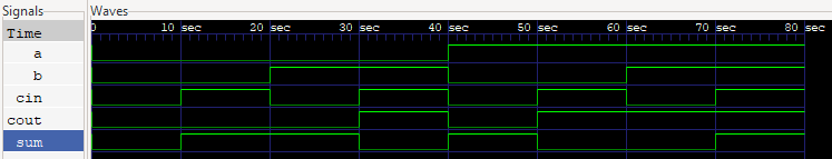 |
|---|
GTKWave snapshot of the signals returned from the full_adder.v testbench. |
Now let's continue with some of the other crucial modules and then we'll create our ALU and test it as well.
Adder
This is a 16-bit adder chaining 16 full-adders without carry-in or carry-out, as per HACK specifications. It's used in the ALU for addition operations. To illustrate the principle of how the half-adders are wired up, below is an image of a 3-bit adder I created in Logisim:
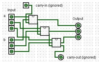 |
|---|
| A 3-bit adder design created in Logisim using full-adders. |
module adder(
    input [15:0] a, b,
    output [15:0] out
);
    wire [16:0] carry;
    assign carry[0] = 1'b0;

    genvar i;
    generate
        for (i = 0; i < 16; i = i + 1) begin : adder_loop
            full_adder fa(
                .a(a[i]),
                .b(b[i]),
                .cin(carry[i]),
                .sum(out[i]),
                .cout(carry[i+1])
            );
        end
    endgenerate
endmodule
Oh, what the heck. You know what? Here is the 16-Bit adder in its full glory as well:
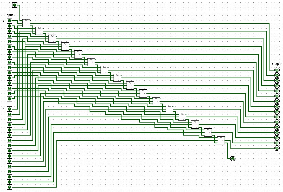 |
|---|
| A 16-bit adder design created in Logisim using full-adders. |
Incrementer
A simple 16-bit incrementer. Here, out = in + 16'd1 assigns the result of in + 16'd1 to the output out where...
in: The 16-bit input vector.16'd1: A 16-bit representation of the decimal number 1. The d indicates that the value is in decimal. It is explicitly specified as 16-bit wide to match the width of the input and output vectors.- And hence
in + 16'd1performs an addition of the input value with the constant value 1.
module incrementer(
    input [15:0] in,
    output [15:0] out
);
    assign out = in + 16'd1;
endmodule
This seems rather simple to implement in Logisim. For example, we may use a 16-Bit adder and simply add 1 with the carry-in bit. Or add one with the second 16-bit number. But this is overly complex as we are essentially wasting 15 input bits and hence also all of the half-adders that would add those two inputs a and b together!
Instead, half-adders to the rescue!
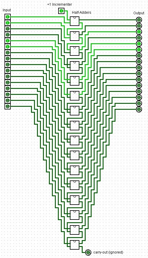 |
|---|
| An incrementer design created in Logisim using half-adders. |
Where before we still had to generate a loop to add together our two 16-Bit numbers together, Verilog simplifies the increment by 1 quite a bit even though we require so many half-adders in our Logisim layout. In Verilog, the high-level abstraction provided by the language allows you to describe the desired behavior of a circuit rather than its specific implementation details, such as using a specific set of half-adders. While structural modeling like I did here in Logisim is important for learning and specific low-level design tasks, behavioral modeling is the preferred approach in most professional design scenarios due to its efficiency and flexibility.
Arithmetic Logic Unit (ALU)
This ALU is specifically designed for the HACK computer and can perform 18 different operations based on the 6 1-bit control bits, which are encoded in the HACK machine language instructions:
zx: Zero the x input
nx: Negate the x input
zy: Zero the y input
ny: Negate the y input
f:  Function select (0 for AND, 1 for ADD)
no: Negate the output
It also has two status outputs:
zr: Set to 1 if the output is zero
ng: Set to 1 if the output is negative (MSB is 1)
The ALU performs operations in stages according to the control bits, allowing for a variety of computations using different combinations of these bits. Here is an implementation in Logisim similar to jbchoinard's sixteen design (GitHub). Instead of using the components we built though, I am using the internal ones in part since their UI is nicer. Sill, you could easily just use the adders we created before.
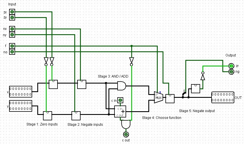 |
|---|
| A full Hack arithmetic logic unit design created in Logisim. |
In Verilog this looks like the code below. I heavily commented this code to explain it:
module alu(
    // This declares the ALU module with its inputs and outputs. The HACK ALU
    // operates on 16-bit numbers (x and y) and has 6 control bits (zx, nx, zy,
    // ny, f, no) that determine its operation.
    // It outputs a 16-bit result (out) and two status flags (zr and ng).
    input [15:0] x, y,              // 16-bit inputs
    input zx, nx, zy, ny, f, no,    // 1-bit inputs
    output [15:0] out,              // 16-bit output
    output zr, ng                   // 1-bit outputs

);
    // These are internal wires used to connect the different stages of the ALU.
    wire [15:0] x1, y1, x2, y2, and_out, add_out, mux_out;

    // Stage 1: Zero inputs
    // If zx is 1, x1 becomes 0, otherwise it's x. Same for y and zy.
    // This implements the "zero" functionality of the HACK ALU.
    assign x1 = zx ? 16'b0 : x;
    assign y1 = zy ? 16'b0 : y;

    // Stage 2: Negate inputs
    // If nx is 1, x2 becomes the bitwise NOT of x1, otherwise it's x1.
    // Same for y2 and ny. This implements the "negate" functionality.
    assign x2 = nx ? ~x1 : x1;
    assign y2 = ny ? ~y1 : y1;

    // Stage 3: AND / ADD
    // This performs both AND and ADD operations on x2 and y2.
    // The HACK ALU always computes both, then selects one based on the f bit.
    assign and_out = x2 & y2;
    adder add(.a(x2), .b(y2), .out(add_out));

    // Stage 4: Choose function
    // If f is 1, the output is the result of addition.
    // If f is 0, it's the result of AND.
    assign mux_out = f ? add_out : and_out;

    // Stage 5: Negate output
    // If no is 1, the output is negated (bitwise NOT).
    assign out = no ? ~mux_out : mux_out;

    // Set zero and negative flags
    // zr is set to 1 if the output is zero.
    // ng is set to 1 if the output is negative (most significant bit is 1).
    assign zr = (out == 16'b0);
    assign ng = out[15];

endmodule
Look at the testbench I wrote in alu.v. Here's what we expect for each case:
x + y: 10 + 5 = 15
x - y: 10 - 5 = 5
y - x: 10 - 5 = 5
x & y: 0b1010101010101010 & 0b1100110011001100 = 0b1000100010001000 (34952)
x | y: 0b1010101010101010 | 0b1100110011001100 = 0b1110111011101110 (61166)
!x: ~0b1010101010101010 = 0b0101010101010101 (21845)
!y: ~0b1010101010101010 = 0b0101010101010101 (21845)
-x: -42 = 65494 (in 16-bit two's complement)
-y: -42 = 65494 (in 16-bit two's complement)
x + 1: 42 + 1 = 43
It returns:
Time=0 x=   10 y=    5 zx=0 nx=0 zy=0 ny=0 f=1 no=0 out=   15 zr=0 ng=0
Time=10 x=   10 y=    5 zx=0 nx=1 zy=0 ny=0 f=1 no=1 out=    5 zr=0 ng=0
Time=20 x=    5 y=   10 zx=0 nx=0 zy=0 ny=1 f=1 no=1 out=    5 zr=0 ng=0
Time=30 x=43690 y=52428 zx=0 nx=0 zy=0 ny=0 f=0 no=0 out=34952 zr=0 ng=1
Time=40 x=43690 y=52428 zx=0 nx=1 zy=0 ny=1 f=0 no=1 out=61166 zr=0 ng=1
Time=50 x=43690 y=    0 zx=0 nx=1 zy=1 ny=0 f=0 no=0 out=    0 zr=1 ng=0
Time=60 x=    0 y=43690 zx=1 nx=0 zy=0 ny=1 f=0 no=0 out=    0 zr=1 ng=0
Time=70 x=   42 y=    0 zx=0 nx=1 zy=1 ny=0 f=1 no=1 out=   42 zr=0 ng=0
Time=80 x=    0 y=   42 zx=1 nx=0 zy=0 ny=1 f=1 no=1 out=   42 zr=0 ng=0
Time=90 x=   42 y=    0 zx=0 nx=1 zy=1 ny=1 f=1 no=1 out=   43 zr=0 ng=0
and
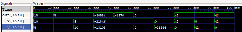 |
|---|
GTKWave snapshot of the signals in signed decimals returned from the alu.v testbench. |
Nice! With that we continue working on the sub-components we need to make sequential changes in our computer, like adding bits to memory and stepping forward in time using a clock.
ALU Operations Table
The HACK ALU's control bits determine which operation is performed. Here are some common operations and their control bit settings:
| Operation | zx | nx | zy | ny | f | no | Description |
|---|---|---|---|---|---|---|---|
| 0 | 1 | 0 | 1 | 0 | 1 | 0 | Constant 0 |
| 1 | 1 | 1 | 1 | 1 | 1 | 1 | Constant 1 |
| -1 | 1 | 1 | 1 | 0 | 1 | 0 | Constant -1 |
| x | 0 | 0 | 1 | 1 | 0 | 0 | Input x |
| y | 1 | 1 | 0 | 0 | 0 | 0 | Input y |
| !x | 0 | 0 | 1 | 1 | 0 | 1 | NOT x |
| !y | 1 | 1 | 0 | 0 | 0 | 1 | NOT y |
| -x | 0 | 0 | 1 | 1 | 1 | 1 | Negate x |
| -y | 1 | 1 | 0 | 0 | 1 | 1 | Negate y |
| x+1 | 0 | 1 | 1 | 1 | 1 | 1 | Increment x |
| y+1 | 1 | 1 | 0 | 1 | 1 | 1 | Increment y |
| x-1 | 0 | 0 | 1 | 1 | 1 | 0 | Decrement x |
| y-1 | 1 | 1 | 0 | 0 | 1 | 0 | Decrement y |
| x+y | 0 | 0 | 0 | 0 | 1 | 0 | Add x and y |
| x-y | 0 | 1 | 0 | 0 | 1 | 1 | Subtract y from x |
| y-x | 0 | 0 | 0 | 1 | 1 | 1 | Subtract x from y |
| x&y | 0 | 0 | 0 | 0 | 0 | 0 | Bitwise AND |
| x | y | 0 | 1 | 0 | 1 | 0 | 1 |
Sequential Logic
The following building blocks, when combined with the ALU and other components, form the complete Hack computer system.
- The D Flip-Flop (DFF) forms the basis for all memory elements.
- The 1-Bit Register is used to construct larger memory units.
- RAM8 and the parameterized RAM are used for data storage.
- And the Counter is used as the program counter in the CPU, like a clock.
DFF
The DFF stores a single bit. On each positive edge of the clock signal, it updates its output q with the value of the input d. Here is a Logisim implementation showing how we can actually store information. From here on out, I will focus on just the Verilog though.
 |
|---|
| A flip-flop circuit storing a bit created in Logisim. |
module DFF(
    input clk,
    input d,
    output reg q
);

always @(posedge clk) begin
    q <= d;
end

endmodule
... Testing with GTKWave ...
1-Bit Register
The 1-Bit Register is a controllable DFF. It stores a single bit and updates its value when the load signal is high. The current state is continuously output.

module Bit(
    input clk,
    input in,
    input load,
    output out
);

reg state;

always @(posedge clk) begin
    if (load)
        state <= in;
end

assign out = state;

endmodule
... Testing with GTKWave ...
8-Register Memory (RAM8)
The RAM8 module is a small memory unit with 8 16-bit registers. It can store a value to a specified address when load is high, and continuously outputs the value at the current address.
module RAM8(
    input clk,
    input [2:0] address,
    input [15:0] in,
    input load,
    output [15:0] out
);

reg [15:0] memory [0:7];

always @(posedge clk) begin
    if (load)
        memory[address] <= in;
end

assign out = memory[address];

endmodule
... Testing with GTKWave ...
n-Register Memory
This is a parameterized RAM module that can be instantiated with different sizes. It functions similarly to RAM8 but with a configurable number of registers. The $clog2(SIZE) determines the width of the address input based on the RAM size.
module RAM(
    input clk,
    input [$clog2(SIZE)-1:0] address,
    input [15:0] in,
    input load,
    output [15:0] out
);

parameter SIZE = 16; // Default size, can be overridden

reg [15:0] memory [0:SIZE-1];

always @(posedge clk) begin
    if (load)
        memory[address] <= in;
end

assign out = memory[address];

endmodule
... Testing with GTKWave ...
Counter
The Counter is a 16-bit program counter for the Hack architecture. It can be reset to 0, loaded with a specific value, or incremented. This is typically used to keep track of the next instruction to be executed in the Hack computer.
module Counter(
    input clk,
    input reset,
    input [15:0] in,
    input load,
    input inc,
    output reg [15:0] out
);

always @(posedge clk) begin
    if (reset)
        out <= 16'b0;
    else if (load)
        out <= in;
    else if (inc)
        out <= out + 1;
end

endmodule
... Testing with GTKWave ...
"The $7 billion Ariane 5 rocket, launched on June 4, 1996, veered off course 40 seconds after launch, broke up, and exploded. The failure was caused when the computer controlling the rocket overflowed its 16-bit range and crashed. The code had been extensively tested on the Ariane 4 rocket. However, the Ariane 5 had a faster engine that produced larger values for the control computer, leading to the overflow." Digital Design and Computer Architetecture by Sarah and David Harris.
You can see why considering the counter and memory is important. And this is one of the reasons we moved on from 16 to 32 to 64 bits. If you have a 64 bit counter, and only ever increment it by 1, you may safely assume it will never overflow since, if your 4 GHz processor increments every single clock cycle, it will still take 146 years to overflow. So in practice: never. Assuming we use off-the-shelve ICs to build a bread board Hack computer. In reality, even this is based on several assumptions that do not apply to modern compute architectures. Having multiples cores, memory allocation optimization, multi-threading, ... I think all of these things break this calculus. That's why certain specialized applications require counters with even 128 bits.
Machine Language
Let's write some Hack assembly language, which is a low-level language designed for the Hack computer.
Introduction to Hack Assembly
... TODO ...
Multiplication Program
This program multiplies the values in R0 and R1, storing the result in R2. It uses a simple repeated addition algorithm. The program loops R1 times, adding R0 to R2 each time, and then decrements R1. This continues until R1 reaches zero.
// Multiplies R0 and R1 and stores the result in R2.
// (R0, R1, R2 refer to RAM[0], RAM[1], and RAM[2], respectively.)

    @R2
    M=0    // Initialize R2 to 0
    @R0
    D=M    // D = R0
    @END
    D;JEQ  // If R0 == 0, goto END

(LOOP)
    @R1
    D=M    // D = R1
    @END
    D;JEQ  // If R1 == 0, goto END
    @R2
    D=M    // D = R2
    @R0
    D=D+M  // D = R2 + R0
    @R2
    M=D    // R2 = R2 + R0
    @R1
    M=M-1  // R1 = R1 - 1
    @LOOP
    0;JMP  // Goto LOOP

(END)
    @END
    0;JMP  // Infinite loop
... Testing ...
I/O-Handling Program
This program demonstrates basic I/O handling in the Hack computer:
It continuously reads from the keyboard (mapped to memory address KBD). If 'T' is pressed, it displays 'T' on the screen (at the memory address SCREEN). If 'q' is pressed, the program ends. For any other key, it continues listening.
// This program reads from the keyboard and displays on the screen.
// It stops when the user presses 'q' (ASCII 113).

(LOOP)
    @KBD
    D=M        // Read from keyboard
    @84
    D=D-A      // Check if 'T' was pressed (ASCII 84)
    @DISPLAY_T
    D;JEQ      // If 'T', goto DISPLAY_T
    @29
    D=D-A      // Check if 'q' was pressed (ASCII 113)
    @END
    D;JEQ      // If 'q', goto END
    @LOOP
    0;JMP      // Otherwise, continue listening

(DISPLAY_T)
    @84
    D=A        // D = 'T'
    @SCREEN
    M=D        // Display 'T' at the top-left of the screen
    @LOOP
    0;JMP      // Go back to listening

(END)
    @END
    0;JMP      // Infinite loop
There are very simple examples but these programs showcase key aspects of Hack assembly:
- Use of A-instructions (@) to set the A register.
- Use of C-instructions for computation and jumps.
- Labels for program flow control.
- Interaction with memory-mapped I/O.
... Testing ...
Computer Architecture
In this chapter, we will create our memory, the CPU, and assemble everything into the complete Hack computer architecture which can load and execute programs!
Memory
Here is the Verilog code for the memory:
module Memory(
    input clk,
    input [14:0] address,
    input [15:0] in,
    input load,
    output [15:0] out
);

    // Declare memory arrays
    reg [15:0] RAM [0:16383];  // 16K RAM
    reg [15:0] SCREEN [0:8191]; // 8K Screen memory

    wire is_ram = (address < 15'h4000);
    wire is_screen = (address >= 15'h4000 && address < 15'h6000);
    wire is_keyboard = (address == 15'h6000);

    reg [15:0] keyboard_state;

    // Memory write operation
    always @(posedge clk) begin
        if (load) begin
            if (is_ram)
                RAM[address] <= in;
            else if (is_screen)
                SCREEN[address - 15'h4000] <= in;
        end
    end

    // Memory read operation
    assign out = is_ram ? RAM[address] :
                 is_screen ? SCREEN[address - 15'h4000] :
                 is_keyboard ? keyboard_state :
                 16'b0;

endmodule
This Memory module represents the main memory of the Hack computer. It includes:
- 16K words of RAM (0x0000 to 0x3FFF)
- 8K words of screen memory (0x4000 to 0x5FFF)
- A single word for keyboard input (0x6000)
Note, 0x means "this is a hexadecimal number" (base 16 instead of base 10). When the computer wants to store or retrieve data, it uses these addresses to know exactly where to go. The CPU can "visit" any of these addresses to read or write data, whether it's general information in the RAM, pixels on the screen, or checking what key was last pressed.
This module also supports both read and write operations, controlled by the 'load' input.
... Testing with GTKWave ...
CPU
As for any von-Neumann architecture, the CPU module is the heart of the Hack computer. It processes instructions and manages the program flow.
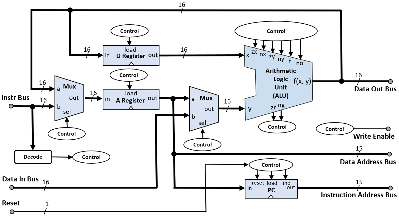 |
|---|
| Hack computer CPU block diagram created by Rleininger, CC BY-SA 4.0. |
Here is the Verilog code:
module CPU(
    input clk,
    input reset,
    input [15:0] inM,
    input [15:0] instruction,
    output [15:0] outM,
    output writeM,
    output [14:0] addressM,
    output [14:0] pc
);

    // Instruction decoding
    wire [15:0] A_Reg, D_Reg, ALU_out;
    wire [5:0] control_bits = instruction[15:10];
    wire [2:0] jump = instruction[2:0];

    // A and D registers
    reg [15:0] A, D;

    // ALU instantiation
    ALU alu(
        .x(D),
        .y(A_Reg),
        .zx(control_bits[5]), .nx(control_bits[4]),
        .zy(control_bits[3]), .ny(control_bits[2]),
        .f(control_bits[1]),  .no(control_bits[0]),
        .out(ALU_out),
        .zr(), .ng()
    );

    // A Register logic
    always @(posedge clk or posedge reset) begin
        if (reset)
            A <= 16'b0;
        else if (!instruction[15] || (instruction[15] && instruction[5]))
            A <= !instruction[15] ? instruction : ALU_out;
    end

    // D Register logic
    always @(posedge clk or posedge reset) begin
        if (reset)
            D <= 16'b0;
        else if (instruction[15] && instruction[4])
            D <= ALU_out;
    end

    // Program Counter logic
    reg [14:0] PC;
    always @(posedge clk or posedge reset) begin
        if (reset)
            PC <= 15'b0;
        else if (/* jump condition */)
            PC <= A[14:0];
        else
            PC <= PC + 1;
    end

    // Output assignments
    assign A_Reg = instruction[15] ? inM : A;
    assign outM = ALU_out;
    assign writeM = instruction[15] && instruction[3];
    assign addressM = A[14:0];
    assign pc = PC;

endmodule
It implements:
- Instruction decoding: Extracts control bits and jump conditions from the instruction.
- A and D registers: Store address and data values respectively.
- ALU: Performs arithmetic and logical operations.
- Program Counter (PC): Keeps track of the next instruction to execute.
The CPU operates in a fetch-decode-execute cycle, updating registers and memory based on the current instruction.
... Testing with GTKWave ...
Instruction Memory
The Instruction Memory module represents the ROM of the Hack computer. So it stores the program instructions and provides them to the CPU based on the address input. The $readmemb system task is used to initialize the ROM with a program file which we feed the program.hack file into:
module InstructionMemory(
    input [14:0] address,
    output reg [15:0] instruction
);

    // ROM to store instructions
    reg [15:0] ROM [0:32767];  // 32K ROM

    // Read instruction from ROM
    always @(*) begin
        instruction = ROM[address];
    end

    // Initialize ROM with program
    initial begin
        $readmemb("program.hack", ROM);
    end

endmodule
... Testing with GTKWave ...
Computer
So finally, this is our complete computer architecture which ties all the previously designed components together:
- CPU: Executes instructions and manages program flow.
- Instruction Memory: Provides instructions to the CPU.
- Data Memory: Stores and retrieves data, including I/O operations.
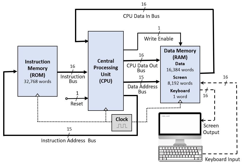 |
|---|
| Hack computer block diagram created by Rleininger, CC BY-SA 4.0. |
module Computer(
    input clk,
    input reset
);

    wire [15:0] inM, instruction, outM;
    wire [14:0] addressM, pc;
    wire writeM;

    // CPU instantiation
    CPU cpu(
        .clk(clk), .reset(reset),
        .inM(inM), .instruction(instruction),
        .outM(outM), .writeM(writeM),
        .addressM(addressM), .pc(pc)
    );

    // Instruction Memory instantiation
    InstructionMemory instr_mem(
        .address(pc),
        .instruction(instruction)
    );

    // Data Memory instantiation
    Memory data_mem(
        .clk(clk),
        .address(addressM),
        .in(outM),
        .load(writeM),
        .out(inM)
    );

endmodule
... Testing with GTKWave ? ...
As such, this module represents the complete Hack computer system. It operates by:
- Fetching instructions from Instruction Memory based on the PC.
- Executing these instructions in the CPU.
- Reading from and writing to Data Memory as needed.
- Updating the PC to move to the next instruction.
A.k.a. the von-Neumann architecture.
Assembler
We'll the high-level language Python to describe the assembler, and Hack assembly language for the example programs. The workflow for now will then be to write a code in Hack, convert it into binary code using our Assembler written in Python, and execute that binary code with our computer.
Writing an Assembler in Python
The assembler I lay out here does two passes. First, we'll record label declarations, then we'll generate binary code, handling both A-instructions and C-instructions. I provide the code for the assembler in the code repository on GitHub. But I encourage you to look at these functions and try to fill it in yourself. It's a simple idea but can be a bit tricky to not make a mistake. In more detail:
- Initializes symbol tables and instruction code tables.
- Removes comments and whitespace from the input.
- Performs a first pass to record label declarations.
- Performs a second pass to generate binary code:
- Handles A-instructions (starting with @)
- Handles C-instructions (dest=comp;jump)
- Writes the resulting binary code to a
.hackfile.
import re
import sys

class Assembler:
    def __init__(self):
        self.symbol_table = {
            'SP': 0, 'LCL': 1, 'ARG': 2, 'THIS': 3, 'THAT': 4,
            'R0': 0, 'R1': 1, 'R2': 2, 'R3': 3, 'R4': 4, 'R5': 5, 'R6': 6, 'R7': 7,
            'R8': 8, 'R9': 9, 'R10': 10, 'R11': 11, 'R12': 12, 'R13': 13, 'R14': 14, 'R15': 15,
            'SCREEN': 16384, 'KBD': 24576
        }
        self.next_variable_address = 16
        self.comp_table = {
            '0': '0101010', '1': '0111111', '-1': '0111010', 'D': '0001100',
            'A': '0110000', '!D': '0001101', '!A': '0110001', '-D': '0001111',
            '-A': '0110011', 'D+1': '0011111', 'A+1': '0110111', 'D-1': '0001110',
            'A-1': '0110010', 'D+A': '0000010', 'D-A': '0010011', 'A-D': '0000111',
            'D&A': '0000000', 'D|A': '0010101',
            'M': '1110000', '!M': '1110001', '-M': '1110011', 'M+1': '1110111',
            'M-1': '1110010', 'D+M': '1000010', 'D-M': '1010011', 'M-D': '1000111',
            'D&M': '1000000', 'D|M': '1010101'
        }
        self.dest_table = {
            '': '000', 'M': '001', 'D': '010', 'MD': '011',
            'A': '100', 'AM': '101', 'AD': '110', 'AMD': '111'
        }
        self.jump_table = {
            '': '000', 'JGT': '001', 'JEQ': '010', 'JGE': '011',
            'JLT': '100', 'JNE': '101', 'JLE': '110', 'JMP': '111'
        }

    def remove_comments_and_whitespace(self, line):
        pass

    def first_pass(self, assembly_code):
        pass

    def get_address(self, symbol):
        pass

    def assemble_a_instruction(self, instruction):
        pass

    def assemble_c_instruction(self, instruction):
        pass

    def second_pass(self, assembly_code):
        pass

    def assemble(self, filename):
        pass

if __name__ == '__main__':
    if len(sys.argv) != 2:
        print("Usage: python assembler.py <input_file.asm>")
        sys.exit(1)

    input_file = sys.argv[1]
    assembler = Assembler()
    assembler.assemble(input_file)
If you use the provided assembler.py script, you can use it from the command line, providing the input .asm file as an argument:
> python assembler.py input_file.asm
The assembler will generate an output file with the same name but with a .hack extension, containing the binary machine code. So let's go back to writing some assembly programs and see what we can make our computer do!
Add
This is one of our two basic arithmetic operations our ALU can do.
// Add.asm
// Computes R0 = 2 + 3

@2
D=A
@3
D=D+A
@0
M=D
Feeding this add.asm file through our assembler, you'll see Hack binary code like add.hack this
0000000000000010
1110110000010000
0000000000000011
1110000010010000
0000000000000000
1110001100001000
created.
In the Hack computer architecture, every line of generated binary code represents one operation or instruction. This is known as a "one instruction per line" or "single instruction per line" architecture.
Note how the assembly code and the generate binary code thus have roughly the same number of lines.
... Testing ...
Max
Compared to the add.asm program, max.asm finding the maximum number of two numbers is a bit longer:
// Max.asm
// Computes R2 = max(R0, R1)

   @R0
   D=M              // D = first number
   @R1
   D=D-M            // D = first number - second number
   @OUTPUT_FIRST
   D;JGT            // if D>0 (first is greater) goto output_first
   @R1
   D=M              // D = second number
   @OUTPUT_D
   0;JMP            // goto output_d
(OUTPUT_FIRST)
   @R0
   D=M              // D = first number
(OUTPUT_D)
   @R2
   M=D              // M[2] = D (greatest number)
(INFINITE_LOOP)
   @INFINITE_LOOP
   0;JMP            // infinite loop
... Testing ...
Rect
Now, the next big goal is to be able to play a game of Pong on our computer. For that, we need to draw images to the screen! The code below shows how to draw a simple rectangle.
// Rect.asm
// Draws a rectangle at the top-left corner of the screen.
// The rectangle is 16 pixels wide and R0 pixels high.

   @0
   D=M
   @INFINITE_LOOP
   D;JLE
   @counter
   M=D
   @SCREEN
   D=A
   @address
   M=D
(LOOP)
   @address
   A=M
   M=-1
   @address
   D=M
   @32
   D=D+A
   @address
   M=D
   @counter
   MD=M-1
   @LOOP
   D;JGT
(INFINITE_LOOP)
   @INFINITE_LOOP
   0;JMP
... Testing ...
Notes & Conclusion
The ideal computer can handle arbitrarily diverse and complicated tasks in parallel. In reality though, there are always trade-offs to be made which is why we develop different architectures most commonly the CPU and the Graphics Processing Unit (GPU). CPUs are great at handling various diverse complicated tasks one by one. GPUs are great at handling the many of the same simple tasks in parallel. But there is much more to modern designs than what I have talked about up until and I want to create a little overview.
Modern CPUs
To summarize this video, below, you can see a schematic overview of a typical CPU with multiple processing cores consisting of a control unit, ALU, and register coupled to various levels of cache memory (SRAM), and including a graphics controller which is typically connected to a GPU and a memory controller which in turn is connected to DRAM memory via a memory bus.
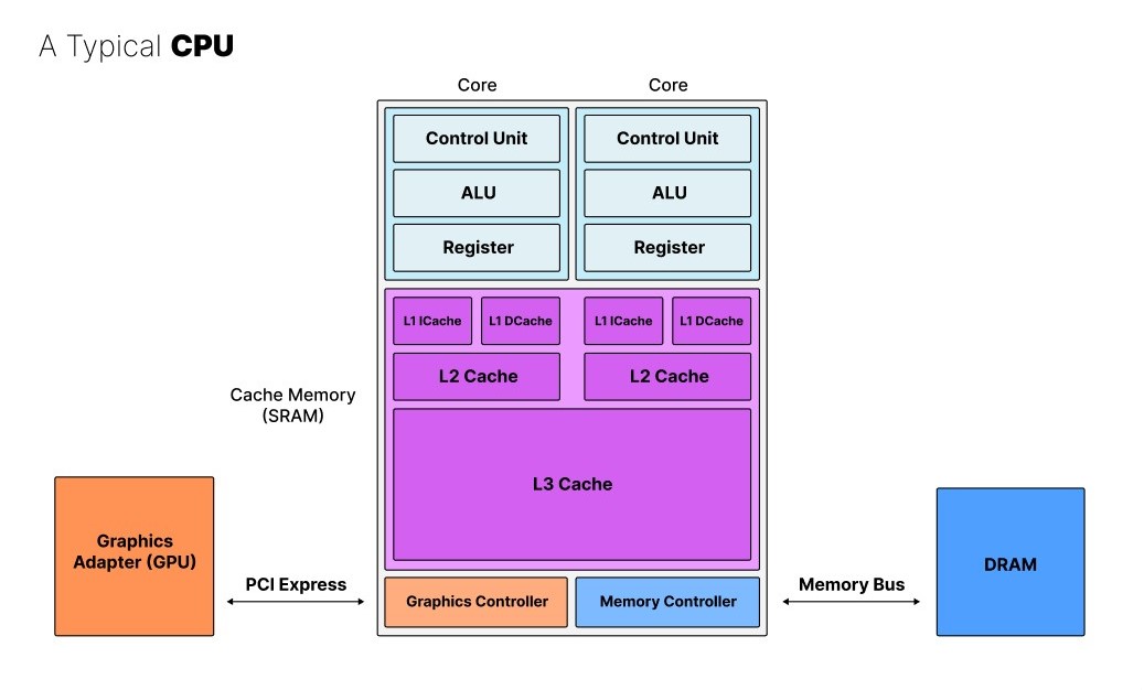 |
|---|
| Schematic overview of a typical modern CPU. |
The different caches operate at varying speeds to distribute data among the cores efficiently. To further optimize the data exchange between the cores and the memory, the L1 cache is split into an instruction cache (ICache) and data cache (DCache). The ICache only writes and hence tells the core which operations to execute while the DCache only writes and reads data to and from the core.
If we compare this with the Hack computer architecture, its minimalism becomes clear. Modern CPUs have much more advanced capabilities. To summarize:
- Branching: Modern CPUs have advanced branching capabilities, which allow them to make decisions and execute different code paths based on various conditions. This is a crucial feature that allows CPUs to handle complex, diverse tasks.
- Multiple Cores: Modern CPUs typically have multiple processing cores, allowing them to execute multiple tasks or threads concurrently, improving overall performance. This became crucial in recent decades as Moore's Law started failing. And it goes much further than the original von-Neumann architecture.
- Hierarchical and More Optimized Cache: As mentioned, modern CPUs have a hierarchical cache system (L1, L2, L3) with specialized instruction and data caches (the so-called Harvard architecture, again, different from the von-Neumann architecture), which helps to efficiently manage and distribute data between the cores and main memory.
- Graphics Controller: Many modern CPUs integrate a graphics controller, which offloads some graphics processing tasks from the main CPU cores, improving overall system performance.
- Larger Instruction Set and More Complex ALU/Control Unit: Modern CPUs have a much larger and more complex instruction set, as well as more advanced Arithmetic Logic Units (ALUs) and Control Units, allowing them to handle a wider range of operations and tasks.
Modern GPUs
Modern graphics are extremely data intensive (hence the PCI Express for greater bandwidth) and demand for parallel compute (hence vast amounts of cores a.k.a. "shader cores"). While there are many cores they all have comparatively simple instructions though. It follows the "Single Instruction, Multiple Data" (SIMD) paradigm. This is possible because there is a much more clear and repetitive pipeline for GPUs. After all, they were originally and are still primarily meant for graphics acceleration. Below, you can see an illustration of the graphics rendering pipeline (as summarized by this video).
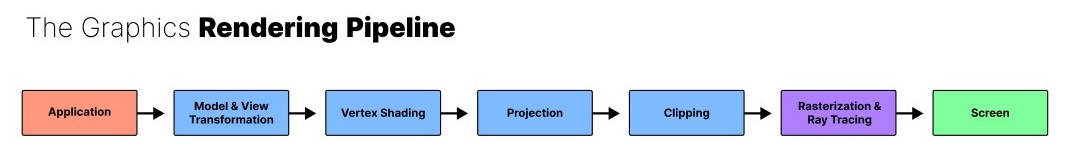 |
|---|
| Schematic overview of a typical GPU's graphics rendering pipeline. |
Note also, that GPUs have no need for registers.
GPUs are quite general these days but they are still primarily optimized to handle graphics. So while they can also run parallel physics or neural networks, a dedicated physics processing unit or dedicated AI accelerators are still outperforming GPUs by a lot. The reason we do not see much of this yet is the ecosystem NVIDIA has built around their graphics cards and monopolizes. Indeed, NVIDIA introduced a dedicated core to solve the computationally heavy task of ray-tracing a few years ago. It will take time to build the software, workflows, hardware, and various integrations etc. for AI accelerators to take over. It will take even longer for this to happen for physics processors given that there is no clearly communicated demand for it on the market right now.
Parallelism: SISD to MIMD
SIMD describes computers with multiple processing elements that perform the same operation on multiple data points simultaneously rather than "Single Instruction, Single Data" (SISD) as in the Hack computer we've built. Below is an illustration of the general idea layed out originally in Flynn's Taxonomy:
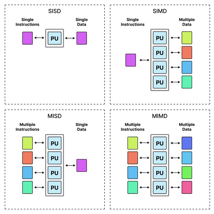 |
|---|
| Flynn's Taxonomy of (parallel) processing with single or multiple data or instructions. |
GPUs are SIMD. And where the original computer and CPU was clearly SISD, modern CPUs, especially those used for supercomputers, are now typically MIMD, so that various different applications with different data can run in parallel. Yet, the complexity of such an architecture only allows for a relatively low number of cores compared to SIMD. Hence, ultra-parellilsm is only really feasable with SIMD.