Computer Engineering: The Arithmetic Logic Unit
Introduction
“On the one hand, the Hack [general computer] architecture can be built in just a few hours of work, […] at the same time, Hack is sufficiently general to illustrate the key operating principles and hardware elements underlying the design of any digital computer.” Elements of Computing Systems (ECS).
If you want to learn how to design a Hack computer and do all of the above, I documented every step of the process in a series of notes / blog posts with this being the first one. This is not a guide to solve the famous NAND-to-Tetris course challenges. I barely skimmed the book and didn’t look at the course much. Nonetheless, I recommend getting this book.
If you actually want to work through this and build your own Hack computer similar to how I did it, we’ll first need to set up our development environment. Feel free to skip this if you already understand Verilog and you’re just want to read/browse a little.
Tools
Only a few tools are necessary. We use
- Visual Studio Code and
- Verilog HDL to program the designs,
- Icarus Verilog for simulation as it is easier to install than Verilator on Windows, and
- GTKWave for waveform viewing.
- And Python for simple scripts like the assembler.
Optionally, Logisim can be a nice playground to test circuit ideas fast.
Installing Logisim
Installing Logisim is as easy as downloading the .exe from http://www.cburch.com/logisim/ and following the install instructions. It is a compiled program with an intuitive GUI. You can then go ahead and immediately build your first digital circuits. In fact, Logisim is quite capable of simulating any computer you want to build. But while it is more intuitive and great for testing ideas, it is also quite time-consuming for larger projects to draw and connect every component yourself. That’s just one of many reasons for why we have programmatic hardware description languages.
Installing Icarus Verilog & GTK Wave
Download Icarus here. This installation program will include gtkwave as well. Make sure to use the most recent version and during installation check the installation path box so that you can open Icarus and verilog simply by typing
>gtkwave
which opens a nice little GUI which we’ll discuss later or
>iverilog
which will just print out some text in your terminal. This video might be of great help to you and it also shows you how to write, simulate, and visualize the signals of your Verilog modules. It really is that simple. The whole ecosystem simply has terrible, terrible documentation.
The Basic Workflow
The workflow overall using these tools is pretty straightforward and we’ll repeat it over and over.
Step 1: Create a Verilog file. We’ll call this one test.v:
module myModule();

initial
  begin
    $display("Hello World!");   // This will display a message
    $finish ; // This causes the simulation to end.  Without, it would go on..and on.
  end

endmodule
This module simply prints out the classic “Hello World!”. Great!
Step 2. We compile the .v file using Icarus:
>iverilog -o test.vvp test.v
The -o switch assigns a name to the output object file. Without this switch the output file would be called a.out. The hello.v indicates the source file to be compiled. There should be practically no output when you compile this source code, unless there are errors.
Step 3. You are ready to simulate this Hello World verilog program. To do so, invoke as such:
>vvp test.vvp
Hello World!
Now, inside Visual Studio Code you can install the Verilog HDL extension which adds a little green button at the top of the window which helps you compile your verilog code instead of you having to type the command out in the terminal every time.
Step 4. Visualize the waveforms/signals in gtkwave to check if our module functions as desired. To create and visualize waveforms, modify your Verilog code to include signal declarations and generate a VCD (Value Change Dump) file. Let’s take for example the following Verilog:
module myModule();
  reg clk;  // Declare a clock signal
  reg [3:0] counter;  // Declare a 4-bit counter

  initial begin
    $dumpfile("test.vcd");  // Create a VCD file named test.vcd
    $dumpvars(0, myModule);  // Dump all variables in the module

    clk = 0;
    counter = 0;

    repeat(16) begin
      #5 clk = ~clk;  // Toggle clock every 5 time units
      if (clk) counter = counter + 1;  // Increment counter on rising edge
    end

    $display("Simulation complete");
    $finish;
  end
endmodule
Compile and run the simulation as before:
>iverilog -o test.vvp test.v
>vvp test.vvp
which now also creates the test.vcd file. Which we can then view with
>gtkwave test.vcd
opening the GTKView software. Select the waveform in the UI and you’ll see something like this:
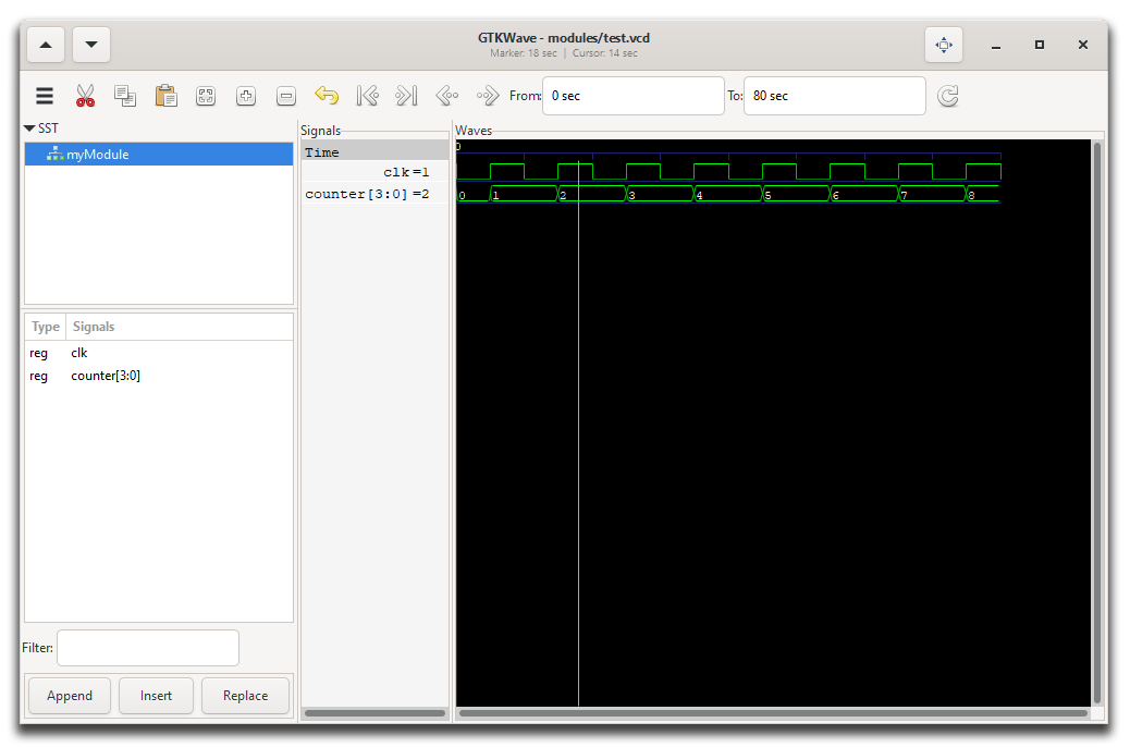
GTKWave program showing the test.vcd waveform.
A Short Introduction to Verilog
Verilog is a hardware description language (HDL) used to model digital electronic systems. It can be used to describe hardware at various levels of abstraction, from high-level behavioral descriptions to low-level gate-level implementations allowing designers to simulate and synthesize digital circuits as hinted at before.
As we already saw as well, the basic unit of design in Verilog is a module which can represent anything from simple print statement or gate to highly complex systems. It has
- a port list (inputs and outputs)
- and a body describing its functionality.
Verilog has two main data types: nets (like wires) and registers.
Common keywords are: wire, reg, integer, real, time.
Vectors can be declared to represent multiple bits (e.g., wire [7:0] bus;).
In this case, we have an 8-bit bus.
And importantly, there are various operations Verilog defines.
| Category | Operator | Name | Description |
|---|---|---|---|
| Bitwise | & |
Bitwise AND | Performs a bitwise AND operation between corresponding bits of two operands. Each bit of the result is set to 1 if both corresponding bits of the operands are 1. |
| Bitwise | \| |
Bitwise OR | Performs a bitwise OR operation between corresponding bits of two operands. Each bit of the result is set to 1 if at least one of the corresponding bits of the operands is 1. |
| Bitwise | ^ |
Bitwise XOR | Performs a bitwise exclusive OR (XOR) operation between corresponding bits of two operands. Each bit of the result is set to 1 if only one of the corresponding bits is 1. |
| Bitwise | ~ |
Bitwise NOT | Performs a bitwise negation (complement) of the operand. It inverts each bit of its operand. |
| Logical | && |
Logical AND | Returns true if both operands are non-zero (true), otherwise returns false. Unlike &, it operates on entire expressions, not individual bits. |
| Logical | \|\| |
Logical OR | Returns true if at least one of the operands is non-zero (true). Similar to &&, it operates on entire expressions. |
| Logical | ! |
Logical NOT | Returns true if the operand is zero (false), otherwise returns false. It inverts the boolean value of its operand. |
| Arithmetic | + |
Addition | Adds two operands. |
| Arithmetic | - |
Subtraction | Subtracts the second operand from the first. |
| Arithmetic | * |
Multiplication | Multiplies two operands. |
| Arithmetic | / |
Division | Divides the first operand by the second operand. Note that in Verilog, division of integers results in integer division. |
| Arithmetic | % |
Modulus | Returns the remainder after division of the first operand by the second. |
| Relational | == |
Equality | Returns true if both operands are equal. |
| Relational | != |
Inequality | Returns true if the operands are not equal. |
| Relational | < |
Less Than | Returns true if the first operand is less than the second. |
| Relational | > |
Greater Than | Returns true if the first operand is greater than the second. |
| Relational | <= |
Less Than or Equal To | Returns true if the first operand is less than or equal to the second. |
| Relational | >= |
Greater Than or Equal To | Returns true if the first operand is greater than or equal to the second. |
| Shift | << |
Logical Left Shift | Shifts the bits of the first operand to the left by the number of positions specified by the second operand. Zeroes are shifted into the lower bits. |
| Shift | >> |
Logical Right Shift | Shifts the bits of the first operand to the right by the number of positions specified by the second operand. Zeroes are shifted into the higher bits. |
| Concatenation | {} |
Concatenation | Combines multiple values or vectors into a single vector. For example, {A, B} concatenates the values A and B into a larger bit vector. |
As I mentioned, we can define quite complex modules. Indeed, there are three different paradigms for how to do so: Procedural Blocks, Behavioral Constructs, and Structural Constructs. But more about that later.
Verilog supports specifying delays and timing constraints where symbol is used for delays in simulation.
Here is a simple example of a more practical Verilog module:
module d_flip_flop (
    input clk,    // Clock input
    input d,      // Data input
    output reg q  // Output
);

always @(posedge clk) begin
    q <= d;
end

endmodule
It describes a D flip-flop that updates its output q with the value of input d on the rising edge of the clock signal clk. So we have two inputs (clk, d) and one output (q). The reg defines the data type as a register. A reg can hold a value between assignments, unlike a wire which does not store values.
Boolean Arithmetic
Let’s build up the individual modules which are typical for ALUs within CPUs, step-by-step. Note that the HACK architecture is extremely simplified. Compare the Verilog I show below to that of other designs and you’ll quickly notice the simplicity.
Open the logic.circ Logisim file from the root directory to try out and experiment with the circuits I present here.
Half-Adder
A half-adder is a digital circuit that adds two single binary digits and produces a sum and a carry. The sum is the XOR of the inputs, while the carry is the AND of the inputs.
Truth table for a half-adder:
| Input A | Input B | Sum | Carry |
|---|---|---|---|
| 0 | 0 | 0 | 0 |
| 0 | 1 | 1 | 0 |
| 1 | 0 | 1 | 0 |
| 1 | 1 | 0 | 1 |
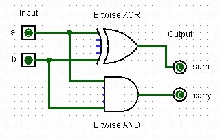
A half-adder design created in Logisim with two input bits, two output bits, one bitwise XOR and one bitwise AND logic gate.
module half_adder(
    input a, b,
    output sum, carry
);
    assign sum = a ^ b;
    assign carry = a & b;
endmodule
Let’s test this baby to see if it actually does what it is supposed to do. For that, we add a little testbench to our previous code like this
module half_adder(
    input a, b,
    output sum, carry
);
    assign sum = a ^ b;
    assign carry = a & b;
endmodule

// Testbench
module half_adder_tb;
    // Declare signals
    reg a, b;
    wire sum, carry;

    // Instantiate the half adder
    half_adder ha1 (.a(a), .b(b), .sum(sum), .carry(carry));

    // Generate VCD file
    initial begin
        $dumpfile("modules/half_adder.vcd");
        $dumpvars(0, half_adder_tb);

        // Test cases
        a = 0; b = 0; #10;
        a = 0; b = 1; #10;
        a = 1; b = 0; #10;
        a = 1; b = 1; #10;

        $finish;
    end

    // Display results
    initial begin
        $monitor("Time=%0t a=%b b=%b sum=%b carry=%b", $time, a, b, sum, carry);
    end
endmodule
Follow the steps for using GTKWave of the previous chapter and you’ll see a return in the terminal and a waveform like this:
VCD info: dumpfile half_adder.vcd opened for output.
Time=0 a=0 b=0 sum=0 carry=0
Time=10 a=0 b=1 sum=1 carry=0
Time=20 a=1 b=0 sum=1 carry=0
Time=30 a=1 b=1 sum=0 carry=1
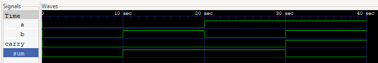
GTKWave snapshot of the signals returned from the half_adder.v testbench.
Does that make sense? Yes! Great. Let’s move on to the next module.
Full-Adder
A full-adder adds three single binary digits (two inputs and one carry-in) and produces a sum and a carry-out. It’s implemented using two half-adders and an OR gate.
Truth table for a full-adder:
| Input A | Input B | Carry In | Sum | Carry Out |
|---|---|---|---|---|
| 0 | 0 | 0 | 0 | 0 |
| 0 | 0 | 1 | 1 | 0 |
| 0 | 1 | 0 | 1 | 0 |
| 0 | 1 | 1 | 0 | 1 |
| 1 | 0 | 0 | 1 | 0 |
| 1 | 0 | 1 | 0 | 1 |
| 1 | 1 | 0 | 0 | 1 |
| 1 | 1 | 1 | 1 | 1 |
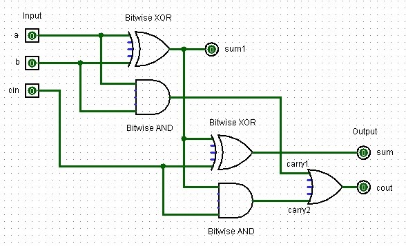
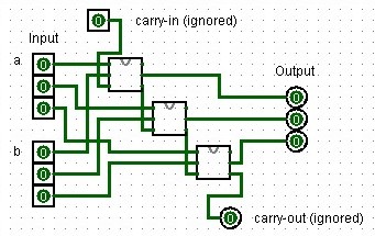
A full-adder design created in Logisim with two input signal bits, one control bit (cin), two output bits, one controt output bit (cout), and several XOR, AND and OR logic gates.
module full_adder(
    input a, b, cin,
    output sum, cout
);
    wire sum1, carry1, carry2;

    half_adder ha1(.a(a), .b(b), .sum(sum1), .carry(carry1));
    half_adder ha2(.a(sum1), .b(cin), .sum(sum), .carry(carry2));

    assign cout = carry1 | carry2;
endmodule
I won’t show you the test bench here but you can see it in the modules directory on Github. The results are as expected:
VCD info: dumpfile modules/full_adder.vcd opened for output.
Time=0 a=0 b=0 cin=0 sum=0 cout=0
Time=10 a=0 b=0 cin=1 sum=1 cout=0
Time=20 a=0 b=1 cin=0 sum=1 cout=0
Time=30 a=0 b=1 cin=1 sum=0 cout=1
Time=40 a=1 b=0 cin=0 sum=1 cout=0
Time=50 a=1 b=0 cin=1 sum=0 cout=1
Time=60 a=1 b=1 cin=0 sum=0 cout=1
Time=70 a=1 b=1 cin=1 sum=1 cout=1
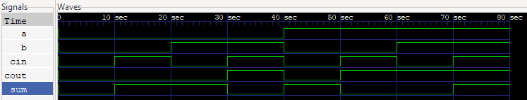
GTKWave snapshot of the signals returned from the full_adder.v testbench.
Now let’s continue with some of the other crucial modules and then we’ll create our ALU and test it as well.
Adder
This is a 16-bit adder chaining 16 full-adders without carry-in or carry-out, as per HACK specifications. It’s used in the ALU for addition operations. To illustrate the principle of how the half-adders are wired up, below is an image of a 3-bit adder I created in Logisim:
A 3-bit adder design created in Logisim using full-adders.
module adder(
    input [15:0] a, b,
    output [15:0] out
);
    wire [16:0] carry;
    assign carry[0] = 1'b0;

    genvar i;
    generate
        for (i = 0; i < 16; i = i + 1) begin : adder_loop
            full_adder fa(
                .a(a[i]),
                .b(b[i]),
                .cin(carry[i]),
                .sum(out[i]),
                .cout(carry[i+1])
            );
        end
    endgenerate
endmodule
Oh, what the heck. You know what? Here is the 16-Bit adder in its full glory as well:
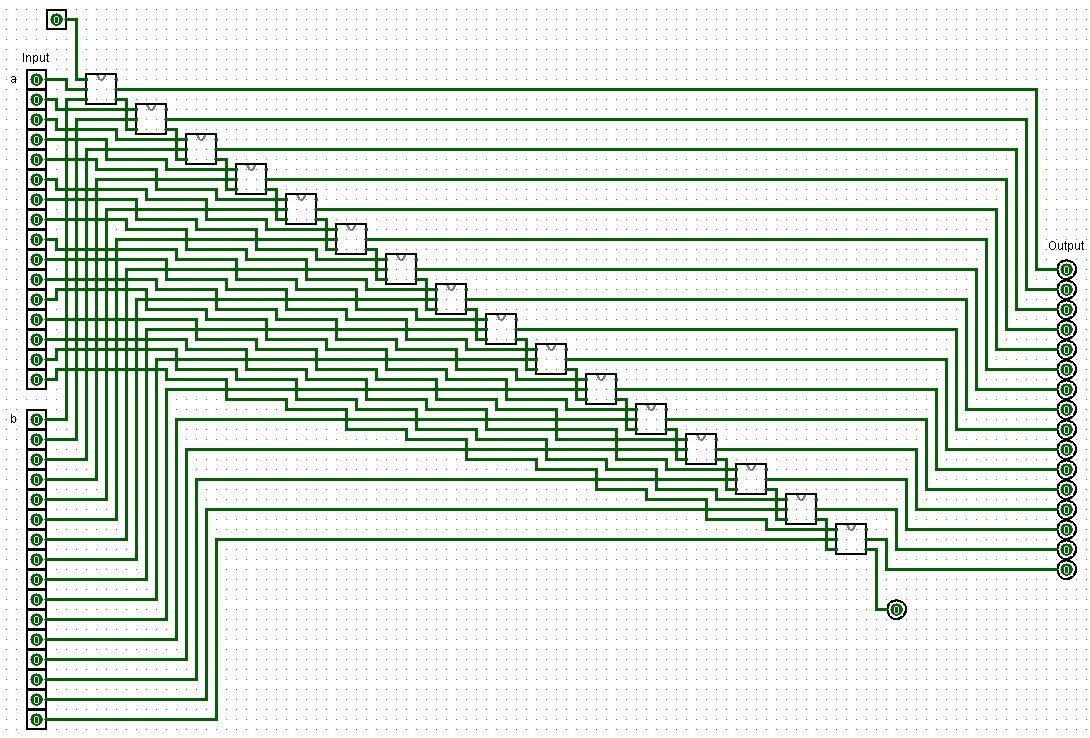
A 16-bit adder design created in Logisim using full-adders.
Incrementer
A simple 16-bit incrementer. Here, out = in + 16'd1 assigns the result of in + 16'd1 to the output out where…
in: The 16-bit input vector.16'd1: A 16-bit representation of the decimal number 1. The d indicates that the value is in decimal. It is explicitly specified as 16-bit wide to match the width of the input and output vectors.- And hence
in + 16'd1performs an addition of the input value with the constant value 1.
module incrementer(
    input [15:0] in,
    output [15:0] out
);
    assign out = in + 16'd1;
endmodule
This seems rather simple to implement in Logisim. For example, we may use a 16-Bit adder and simply add 1 with the carry-in bit. Or add one with the second 16-bit number. But this is overly complex as we are essentially wasting 15 input bits and hence also all of the half-adders that would add those two inputs a and b together!
Instead, half-adders to the rescue!
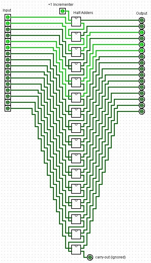
An incrementer design created in Logisim using half-adders.
Where before we still had to generate a loop to add together our two 16-Bit numbers together, Verilog simplifies the increment by 1 quite a bit even though we require so many half-adders in our Logisim layout. In Verilog, the high-level abstraction provided by the language allows you to describe the desired behavior of a circuit rather than its specific implementation details, such as using a specific set of half-adders. While structural modeling like I did here in Logisim is important for learning and specific low-level design tasks, behavioral modeling is the preferred approach in most professional design scenarios due to its efficiency and flexibility.
Arithmetic Logic Unit (ALU)
This ALU is specifically designed for the HACK computer and can perform 18 different operations based on the 6 1-bit control bits, which are encoded in the HACK machine language instructions:
zx: Zero the x input
nx: Negate the x input
zy: Zero the y input
ny: Negate the y input
f:  Function select (0 for AND, 1 for ADD)
no: Negate the output
It also has two status outputs:
zr: Set to 1 if the output is zero
ng: Set to 1 if the output is negative (MSB is 1)
The ALU performs operations in stages according to the control bits, allowing for a variety of computations using different combinations of these bits. Here is an implementation in Logisim similar to jbchoinard’s sixteen design (GitHub). Instead of using the components we built though, I am using the internal ones in part since their UI is nicer. Sill, you could easily just use the adders we created before.
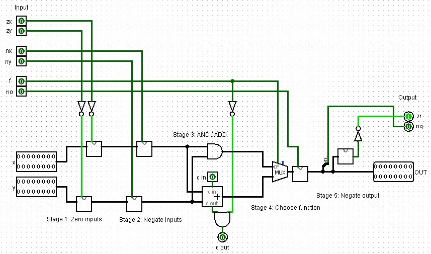
A full Hack arithmetic logic unit design created in Logisim.
In Verilog this looks like the code below. I heavily commented this code to explain it:
module alu(
    // This declares the ALU module with its inputs and outputs. The HACK ALU
    // operates on 16-bit numbers (x and y) and has 6 control bits (zx, nx, zy,
    // ny, f, no) that determine its operation.
    // It outputs a 16-bit result (out) and two status flags (zr and ng).
    input [15:0] x, y,              // 16-bit inputs
    input zx, nx, zy, ny, f, no,    // 1-bit inputs
    output [15:0] out,              // 16-bit output
    output zr, ng                   // 1-bit outputs

);
    // These are internal wires used to connect the different stages of the ALU.
    wire [15:0] x1, y1, x2, y2, and_out, add_out, mux_out;

    // Stage 1: Zero inputs
    // If zx is 1, x1 becomes 0, otherwise it's x. Same for y and zy.
    // This implements the "zero" functionality of the HACK ALU.
    assign x1 = zx ? 16'b0 : x;
    assign y1 = zy ? 16'b0 : y;

    // Stage 2: Negate inputs
    // If nx is 1, x2 becomes the bitwise NOT of x1, otherwise it's x1.
    // Same for y2 and ny. This implements the "negate" functionality.
    assign x2 = nx ? ~x1 : x1;
    assign y2 = ny ? ~y1 : y1;

    // Stage 3: AND / ADD
    // This performs both AND and ADD operations on x2 and y2.
    // The HACK ALU always computes both, then selects one based on the f bit.
    assign and_out = x2 & y2;
    adder add(.a(x2), .b(y2), .out(add_out));

    // Stage 4: Choose function
    // If f is 1, the output is the result of addition.
    // If f is 0, it's the result of AND.
    assign mux_out = f ? add_out : and_out;

    // Stage 5: Negate output
    // If no is 1, the output is negated (bitwise NOT).
    assign out = no ? ~mux_out : mux_out;

    // Set zero and negative flags
    // zr is set to 1 if the output is zero.
    // ng is set to 1 if the output is negative (most significant bit is 1).
    assign zr = (out == 16'b0);
    assign ng = out[15];

endmodule
Look at the testbench I wrote in alu.v. Here’s what we expect for each case:
x + y: 10 + 5 = 15
x - y: 10 - 5 = 5
y - x: 10 - 5 = 5
x & y: 0b1010101010101010 & 0b1100110011001100 = 0b1000100010001000 (34952)
x | y: 0b1010101010101010 | 0b1100110011001100 = 0b1110111011101110 (61166)
!x: ~0b1010101010101010 = 0b0101010101010101 (21845)
!y: ~0b1010101010101010 = 0b0101010101010101 (21845)
-x: -42 = 65494 (in 16-bit two's complement)
-y: -42 = 65494 (in 16-bit two's complement)
x + 1: 42 + 1 = 43
It returns:
Time=0 x=   10 y=    5 zx=0 nx=0 zy=0 ny=0 f=1 no=0 out=   15 zr=0 ng=0
Time=10 x=   10 y=    5 zx=0 nx=1 zy=0 ny=0 f=1 no=1 out=    5 zr=0 ng=0
Time=20 x=    5 y=   10 zx=0 nx=0 zy=0 ny=1 f=1 no=1 out=    5 zr=0 ng=0
Time=30 x=43690 y=52428 zx=0 nx=0 zy=0 ny=0 f=0 no=0 out=34952 zr=0 ng=1
Time=40 x=43690 y=52428 zx=0 nx=1 zy=0 ny=1 f=0 no=1 out=61166 zr=0 ng=1
Time=50 x=43690 y=    0 zx=0 nx=1 zy=1 ny=0 f=0 no=0 out=    0 zr=1 ng=0
Time=60 x=    0 y=43690 zx=1 nx=0 zy=0 ny=1 f=0 no=0 out=    0 zr=1 ng=0
Time=70 x=   42 y=    0 zx=0 nx=1 zy=1 ny=0 f=1 no=1 out=   42 zr=0 ng=0
Time=80 x=    0 y=   42 zx=1 nx=0 zy=0 ny=1 f=1 no=1 out=   42 zr=0 ng=0
Time=90 x=   42 y=    0 zx=0 nx=1 zy=1 ny=1 f=1 no=1 out=   43 zr=0 ng=0
and
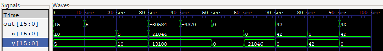
GTKWave snapshot of the signals in signed decimals returned from the alu.v testbench.
Nice! With that we continue working on the sub-components we need to make sequential changes in our computer, like adding bits to memory and stepping forward in time using a clock.
The HACK ALU’s control bits determine which operation is performed. Here are some common operations and their control bit settings:
| Operation | zx | nx | zy | ny | f | no | Description |
|---|---|---|---|---|---|---|---|
| 0 | 1 | 0 | 1 | 0 | 1 | 0 | Constant 0 |
| 1 | 1 | 1 | 1 | 1 | 1 | 1 | Constant 1 |
| -1 | 1 | 1 | 1 | 0 | 1 | 0 | Constant -1 |
| x | 0 | 0 | 1 | 1 | 0 | 0 | Input x |
| y | 1 | 1 | 0 | 0 | 0 | 0 | Input y |
| !x | 0 | 0 | 1 | 1 | 0 | 1 | NOT x |
| !y | 1 | 1 | 0 | 0 | 0 | 1 | NOT y |
| -x | 0 | 0 | 1 | 1 | 1 | 1 | Negate x |
| -y | 1 | 1 | 0 | 0 | 1 | 1 | Negate y |
| x+1 | 0 | 1 | 1 | 1 | 1 | 1 | Increment x |
| y+1 | 1 | 1 | 0 | 1 | 1 | 1 | Increment y |
| x-1 | 0 | 0 | 1 | 1 | 1 | 0 | Decrement x |
| y-1 | 1 | 1 | 0 | 0 | 1 | 0 | Decrement y |
| x+y | 0 | 0 | 0 | 0 | 1 | 0 | Add x and y |
| x-y | 0 | 1 | 0 | 0 | 1 | 1 | Subtract y from x |
| y-x | 0 | 0 | 0 | 1 | 1 | 1 | Subtract x from y |
| x&y | 0 | 0 | 0 | 0 | 0 | 0 | Bitwise AND |
| x|y | 0 | 1 | 0 | 1 | 0 | 1 | Bitwise OR |
Conclusion
In this first post, we’ve established the foundation for building a complete Hack computer from scratch. We set up our development environment with Logisim, Icarus Verilog, and GTKWave, then explored Verilog fundamentals including data types, module structure, and the comprehensive operator set. Most importantly, we built the essential arithmetic circuits that form the core of any computer: half-adders, full-adders, a 16-bit adder, an incrementer, and finally a complete ALU capable of 18 different operations.
If I ever get around to polishing up my notes, we’ll tackle sequential logic and memory systems in the next post, then move on to CPU architecture and control units. Eventually, we’ll create an assembler and integrate everything into a working computer.